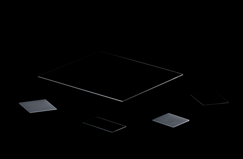


Silicon on Sapphire
As a professional sapphire wafer manufacturer, CRYSCORE can provide standard or optical sapphire wafers with any orientation applied to epitaxy, as well as sapphire windows with any specifications applied to optics. Patterned sapphire substrates and sapphire ingots also can be provided. Expert in sapphire optics manufacturing.
SILICON ON SAPPHIRE
A Brief Introduction of Silicon on Sapphire Technology
Silicon on sapphire (SOS) technology is a hetero-epitaxial process for metal-oxide-semiconductor (MOS) integrated circuit (IC) manufacturing that consists of a thin layer (typically thinner than 0.6 µm) of silicon grown on a SOS wafer (Al2O3). SOS wafers are part of the silicon-on-insulator (SOI) family of CMOS (complementary MOS) technologies. Typically, high-purity artificially grown sapphire crystals are used.
The silicon is usually deposited by the decomposition of silane gas (SiH4) on heated sapphire substrates. The advantage of sapphire is that it is an excellent electrical insulator, preventing stray currents caused by radiation from spreading to nearby circuit elements. SOS faced early challenges in commercial manufacturing because of difficulties in fabricating the very small transistors used in modern high-density applications.
This is because the SOS process results in the formation of dislocations, twinning and stacking faults from crystal lattice disparities between the sapphire and silicon. Additionally, there is some aluminum, a p-type dopant, contamination from the substrate in the silicon closest to the interface.
Silicon on Sapphire Technology
Why is Silicon on Sapphire Technology So Important to Integrated Circuit
Due to sapphire has high permittivity that can eliminate the interaction between components of the integrated circuit, not only can reduce leakage current and parasitic capacitance, enhance radiation resistance and reduce power consumption but also can improve the level of integration and two-layer wiring, thus, sapphire is the ideal material for large scale and very large scale integrated circuit.
Silicon on sapphire technology provides ideal isolation and reduces the parasitic capacitance at the bottom of the PN junction, so it is suitable for high-speed large scale integrated circuits to achieve high speed and low power consumption. This process is generally used to make CMOS circuits.
In addition, in the SOS microelectronic circuit design and production, all kinds of semiconductor devices usually need to make on the structural integrity silicon thin film, and because thermal expansion coefficient of silicon is similar to sapphire, a silicon monocrystalline film (100) can be grown on the surface orientation(1-102) of the sapphire substrate by heteroepitaxy.
At present, sapphire crystal has become a widely used substrate for the growth of semiconductor materials.
Contact : Zhu Wind, +86 0391 393 3936
Good deal: buying from seller
We invite you to read our terms of use. You can also visit our FAQ section and see our information section on the risks associated with counterfeiting.
|
This page is about importers and exporters of Silicon on Sapphire Search in a category : Second hand goods Search in a category : silicon, sapphire |
Report abuse
Thursday, August 06, 2015
Quantity : 30 sets
Manual type & CNC Drilling EDM profession manufacturer. Drilling capacity dia. is fromФ0.1mm to Ф6.0mm. High verticality (deviation) is lower than 0.03. Inbuilt water filtration system and pure water available. Ion Exchange Resin Treatment Filter support more machines and...
Sane Kuei Machinery Co., Ltd
- Sane Kuei Machinery Co., Ltd
- 24158 - New Taipei City
- +886285112370
Report abuse

Saturday, August 23, 2014
Détails sur mesure de meubles LED 1 La luminosité de la source de lumière LED 2 temps de la batterie de travail: tous nos meubles conduit peut être utilisé 8-10 heures après une charge complète, mais plus de 12 heures peut être personnalisé. 3. différentes fonctions: comme DMX...
Report abuse
Tuesday, October 02, 2012
Cartes pour l'export sur les pays de l'Ouest Afrique Sub Saharienne Je prépare une mission dans cette zone. Le but est d'optimiser cette mission en trouvant les meilleurs contacts possibles sur place (bureaux d'études, installateurs HVAC et clients grands comptes directs) Le départ...
JEAN LUC MARTIN
- 97434 - SAINT GILLES
- 06 92 27 49 39
- 02 62 33 95 44