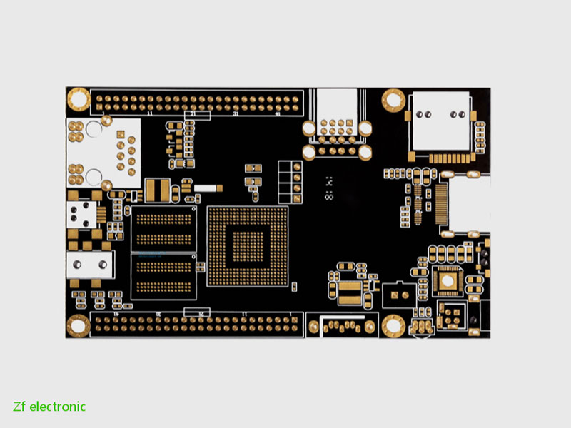


Buried Via PCB
PCBA is a process requiring knowledge covering PCB manufacturing assembly, PCB design, fabrication and a strong understanding of the final product. ZF is a professional pcb manufacturing companies with high-quality, all of our products have obtained ISO9001, ISO13485: 2016, IATF16949: 2016, IPC-A-610E, UL, RoHS certifications.
A buried via is a connection of any circuit layer inside the PCB but not connected to the outer layer. The via cannot be drilled after bonding because it must be drilled on the individual circuit layers first. After partially bonding the inner layer, it has to be plated before finishing the bonding, which is more laborious and therefore more expensive than the original through via and blind via. Usually, it is only used in high-density(HDI) PCB to increase the available space for other circuit layers.
1. What is via?
The via is an important factor in the design of multi-layer PCB and consists of three main parts, including drill hole, the pad around the hole and the POWER layer. When talking about its process, it should be firstly plated a layer of metal by chemical deposition on the cylindrical surface of the via wall to connect the copper foils that need to be connected to the middle layers. The upper and lower sides of the via will be made into a common pad shape, which can be directly connected with the lines near the two sides or not.
2. Classification of vias by function
In terms of function, vias can be divided into two categories. One is used for electrical connection between layers while the other is used for fixing or positioning devices. As for the process, the vias can be generally divided into blind via, buried via and through via.
(1) Blind via
Blind via hole is located on the top and bottom surfaces of the PCB with a certain depth. It is used to connect the line on the surface and the underlying inner line and its depth usually does not exceed a certain ratio (aperture).
(2) Buried via
It refers to the connection via that is in the inner layer of buried via PCB which will not extend to the surface of the circuit board.
Both of above-mentioned two types of vias are located in the inner layers of the circuit board, which are completed by using a through-via forming process before lamination. There may also be several inner layers overlapping during the via formation process.
(3) Through via
The through hole vias penetrate the entire circuit board and can be used for internal interconnection or as a positioning via of component installation. Because of its easier implementation and lower cost in the process, most of the PCBs use it instead of the other two kinds of vias.
The advantages of the blind via and buried via
In the non-through-via technology, the application of blind via and buried via can greatly reduce the size and weight, as well as the number of layers and costs in printing circuit boards, moreover, improve the electromagnetic compatibility, increase the characteristics of electronic products, making the design simpler and faster.
As for the traditional PCB design and processing, there are many problems brought by through vias. First of all, through-vias occupy a large amount of effective space. Secondly, a lot of through-vias densely packed in one place also make the wiring of the inner layers in the multilayer PCB difficult. That is because they will take up the space required for alignment, destroy the impedance characteristics of the power supply and make the power ground plane ineffective. What's worse, the conventional mechanical method of drilling will be 20 times the workload of non-through hole technology.
If you have questions about our buried via PCB production capacity, or the specifications required for your custom project are not listed on this page, please feel free to contact us. We will reply within one workday. We will continue to provide quotation support and design support. Welcome to learn about our production process.
Contact : He Mike, +86 188 7956 1688
Good deal: buying from seller
We invite you to read our terms of use. You can also visit our FAQ section and see our information section on the risks associated with counterfeiting.
|
This page is about importers and exporters of Buried Via PCB Search in a category : Vehicles Search in a category : buried |
Report abuse
Wednesday, September 14, 2016
Quantity : 5000 - Price : 100,00 €
Bellows Seal Stop Valves (Angle Type) DIN Angle Type Bellows Sealed Stop Valve DIN Bellows Seal Globe Valve DIN Faltenbalgventil Eckform DIN Válvulas de fuelle(Paso angular.) DIN ventil uzavírací s vlnovcem rohový DIN Standard seteventil med belg (Vinkel modell) DIN Standardında...
ETM Armaturen
- 59590 - Henri Durre
- 86 577 67953935
Report abuse

Tuesday, July 07, 2026
Quantity : 30 - Price : 328 USD
Complete Factory Audits / Factory Inspections The aim of a factory audit is to confirm that your factory has the production capacity, capability and quality to meet your production needs. Our highly qualified auditors inspect the factory thorough fully. They carry out a comprehensive...
Web Commerce Worldwide
- webcommerceworldwide
- 26250 - Livron Sur Drôme
- +33 4 75 78 05 28
- +33 6 47 31 66 61
Report abuse

Thursday, September 27, 2012
Quantity : conference - Price : conference with clie
This Auto Stainer provides fast, easy and stable staining process for staining sputum specimen (for detecting Tubercle Bacillus) according to Fluorochrome staining method by automated system control. This new innovated stainer features advanced functions and performances over manual...
Dagatronics Corporation
- 411-808 - Geonggi-do
- +82 3 19 16 80 05