 |
|
|
Equipment goods
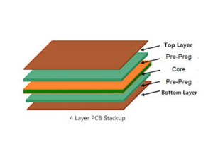
4 Layer PCB
|
|
This page is about importers and exporters of 4 Layer PCB Search in a category : Equipment goods Search in a category : layer |
Tuesday, August 05, 2014
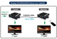
DD1000TR Display Port Chainable Extender over CAT.5e/6 The DD1000TR is the latest high performance, cost-effective Displayport Daisy-Chainable Extender over CAT.5e/6, extended up to 100m between. supports Full HD 1080p, 1920x1080, video and daisy-chainable with high flexibility...
ACAFA Information Co.
- epanio
- 335 - Dasi Township
- +88 6 33 07 13 00
Tuesday, May 20, 2014
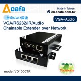
VD1000TR is the latest high performance, cost-effective VGA Daisy-Chainable Extender over CAT.5e/6 with RS-232 IR Audio, extended up to 100m between. VD1000TR supports Full HD 1080p,1920x1080, video and daisy-chainable with high flexibility of expansion as consecutive linking...
ACAFA Information Co.
- epanio
- 335 - Dasi Township
- +88 6 33 07 13 00
Tuesday, May 20, 2014
Quantity : 1000 - Price : N/A
TV150A VGA KVM Chainable Extender over IP with Audio is the innovative solution applied for a wide variety of HID devices extending in terms of excellent compatibility of “True USB emulation” technique, even supports the latest 10- point touch screen, and signals extended...
ACAFA Information Co.
- epanio
- 335 - Dasi Township
- +88 6 33 07 13 00


