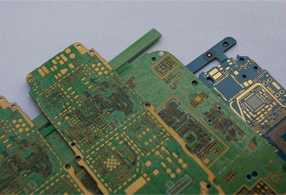
HDI PCB / BLIND&BURIED VIA HOLE PCB / BVH PCB
|
|||||||||||||||||||||||||||||||||||||||||||||||||||||||||||||||||||||||||||||||||||||||||||||||||||||||||||||||||||||||||


|
Items |
Capability. |
|
|
Max board size |
580X700mm |
|
|
Boar Material |
FR-4,Aluminum, High Tg FR4,CEM3,etc. |
|
|
Min trace width/ space (inner layer) |
4mil/4mil(0.1mm/0.1mm) |
|
|
Min PAD (inner layer) |
5 mil(0.13mm) |
|
|
Min thickness(inner layer) |
4 mil(0.1mm) |
|
|
Inner copper thickness |
0.5~4 oz |
|
|
Outer copper thickness |
0.4~6 oz |
|
|
Finished board thickness |
0.4-3.2 mm |
|
|
Board thickness tolerance control |
±0.10 mm |
±0.10 mm |
|
±10% |
±10% |
|
|
±10% |
±10% |
|
|
Inner layer treatment |
brown oxidation |
|
|
Layer count Capability |
1-30 LAYER |
|
|
alignment between ML |
±2mil |
|
|
Drill hole diameter |
0.15mm-0.65mm |
|
|
Aspect ratio of plated hole |
10: 01 |
|
|
Hole precision |
±2 mil(±0.05mm) |
|
|
tolerance for Slot |
±3 mil(±0.75mm) |
|
|
Hole diameter tolerance(PTH) |
±3 mil(±0.075mm) |
|
|
Hole diameter tolerance(NPTH) |
±1mil(±0.025mm) |
|
|
Max Aspect Ratio for PTH |
8: 01 |
|
|
Hole wall copper thickness |
15-50um |
|
|
Alignment of outer layers |
4mil/4mil |
|
|
Min trace width/space for outer layer |
4mil/4mil |
|
|
Tolerance of Etching |
+/-10% |
|
|
Thickness of solder mask |
on trace |
|
|
Thickness of solder mask |
at trace corner |
≥0.2mil(5um) |
|
Hardness of solder mask |
On base material |
≤+1.2mil |
|
6H |
Finished thickness |
|
|
Alignment of solder mask film |
±2mil(+/-50um) |
|
|
Min width of solder mask bridge |
4mil(100um) |
|
|
Max hole with solder plug |
0.5mm |
|
|
Surface treatment |
HAL (Lead or Lead free), immersion Gold, Immersion Nickel, Electric Gold finger, plated Gold, OSP, Immersion Silver.carbon oil,etc. |
|
|
Max Nickel thickness for Gold finger |
280u"(7um) |
|
|
Max gold thickness for Gold finger |
30u"(0.75um) |
|
|
Nickel thickness in Immersion Gold |
120u"/240u"(3um/6um) |
|
|
Gold thickness in Immersion Gold |
2u"/6u"(0.05um/0.15um) |
|
|
Impedance control and its tolerance |
50±10%,75±10%,100±10% 110±10% |
|
|
Trace Anti-stripped strength |
≥61B/in(≥107g/mm) |
|
|
bow and twist |
0.75% |
|
We provide printed circuit board supplies,hdi pcb board,hdi printed circuit boards,hdi pcb prototype,hdi circuit boards,high density interconnect pcb,high density pcb,buried via pcb and buried vias pcb,RFQ today.
Contact : Molly Tu speedapcb, +86 0731 15387574935
Good deal: buying from seller
We invite you to read our terms of use. You can also visit our FAQ section and see our information section on the risks associated with counterfeiting.
|
This page is about importers and exporters of HDI PCB / BLIND&BURIED VIA HOLE PCB / BVH PCB Search in a category : Everything else / Bulk Search in a category : blind&buried, hole |
Report abuse

Saturday, August 23, 2014
Détails sur mesure de meubles LED 1 La luminosité de la source de lumière LED 2 temps de la batterie de travail: tous nos meubles conduit peut être utilisé 8-10 heures après une charge complète, mais plus de 12 heures peut être personnalisé. 3. différentes fonctions: comme DMX...
Report abuse
Friday, October 17, 2014
Quantity : MOQ: 10 - Price : USD 13 - USD 19
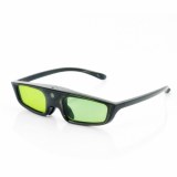
3D Glasses with Active Shutter have been exclusively designed to work with 3D Projections to provide the wearer a real feel of 3D entertainment. Love 3D? Then you will love these active shutter 3D glasses that have been designed to work with 3D DLP projectors. The reason for these...
Pong Yuen Holdings Limited
- pongyuen
- 000000 - Hong Kong
- +85 2 23 65 88 10
- (86)15018920105
Report abuse
Friday, March 04, 2016
Quantity : 150 - Price : 550,00 €
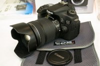
PRODUCT HIGHLIGHTS 20.2MP APS-C CMOS Sensor DIGIC 5+ Image Processor 3.0" 1.04m-Dot Vari-Angle Touchscreen Full HD 1080p/30 Video & Movie Servo AF Dual Pixel CMOS AF with Live View 19-Point All Cross-Type Phase-Detect AF Native ISO 12800, Extended to ISO 25600 7 fps Shooting...
Electronics Design Services
- CM23 2JP - Hertfordshire
- +447405858765