 |
|
|
Equipment goods
Blind & Buried VIA Hole PCB |
|
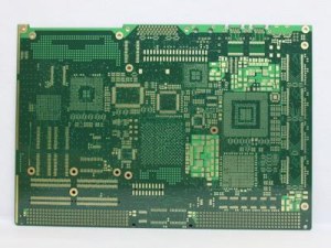
This page is about importers and exporters of Blind & Buried VIA Hole PCB Search in a category : Equipment goods Search in a category : blind, buried, hole |
Thursday, August 25, 2016
Quantity : negotiate - Price : $20-$40
Item name: Cold storage use led light fixture with hole for connect cable conduit Why choose us Water resistant linear vapor-tight fixture,led tri-proof ceiling lights Product Description Water resistant linear vapor-tight fixture,led tri-proof ceiling lights ♦ Product basic...
Jiangmen OGJG Lighting And Electronic Co.,Ltd
- 529095 - Hetang
- 86 750 3715835
Friday, December 11, 2015
Quantity : ask - Price : ask
Health and Beauty care pressotherapy far infrafred carbon fiber material massage bed Longterm treatment is contributed to physical and mental health. Massage can relax muscles,reduce fatigue, relieve stress, improve body blood circulation, enhance physical fitness,aerobics aging...
Guangzhou Yihao Electronic Technology Co., Ltd.
- eho1045
- 510385 - liwan district
- 8602081494207
Friday, November 13, 2015
Quantity : ask - Price : ask
2015 Best selling products in america ! carbon fiber material pressotherapy infrared massage bed Long-term treatment is contributed to physical and mental health. Massage can relax muscl es, reduce fatigue, relieve stress, improve body blood circulation, enhance physical fitness...
Guangzhou Yihao Electronic Technology Co., Ltd.
- eho1045
- 510385 - liwan district
- 8602081494207


