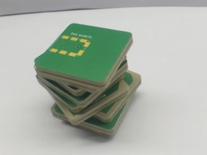
Custom high frequency pcb from professional high frequency pcb company china shenzhen with factory price in low cost.
The high frequency of electronic equipment is a development trend, especially in the development of wireless networks and satellite communications, the high-speed and high-frequency information products, and the standardization of voice, video and data for wireless transmissions with large capacity and fast communication products. A new generation of products that require high-frequency substrates. High Frequency PCB, HF PCB Types as below:
High Frequency PCB Features
1, the impedance control requirements are more stringent, the relative line width control is very strict, the general tolerance is about 2%.
2. Due to the special plate, the adhesion of PTH to copper is not high. It is usually necessary to roughen the via and surface by means of plasma processing equipment to increase the adhesion of PTH hole copper and solder resist ink.
3, can not be used before the resistance welding, otherwise the adhesion will be very poor, can only be roughened with micro-etching water.
4. Most of the plates are made of PTFE. There are many burrs formed by ordinary milling cutters, and special milling cutters are required.
5. The high-frequency PCB is a special circuit board with a high electromagnetic frequency. Generally, the high frequency can be defined as a frequency above 1 GHz.
Its physical properties, precision, and technical parameters are very high, and it is often used in automotive anti-collision systems, satellite systems, radio systems and other fields.
In general terms, the PCB industry considers an RF circuit board to be any high frequency PCB that operates above 100MHz. Within the radio frequency class, anything above 2GHz is a Microwave PCB.
A High Frequency PCB Requires the Use of Specialized Materials
Special materials are required to achieve the high frequency provided by this type of printed circuit board - any changes in the Er value of these materials can affect the impedance of the board. Many PCB designers turn to Rogers dielectric material for its lower dielectric loss, reduced signal loss, lower cost of circuit fabrication and better suitability for fast-turnaround prototyping applications.
Apart from choosing the appropriate PCB material and determining the correct the value of the Er, designers should take parameter such as conductor width and spacing, substrate constant into consideration. These parameters must be exactly specified and implemented with the highest level of process control.
Location : Building 1, Huaide Cuigang Industrial Zone 3, Fuyong Street, Baoan District , Shenzhen, Guangdong 518103, China , 518103 Fuyong Street,
Contact : Mo Jack, +15 9 76 88 36 32


